Article
10 minute read 30 November 2022

AI in chip design: Semiconductor companies are using AI to design better chips faster, cheaper, and more efficiently

Recent advances in machine learning are allowing chip companies to solve one of the biggest design problems ever: How do you arrange 100 billion transistors on one square inch?

Jeff Loucks

Jeff Loucks

United States

Duncan Stewart

Duncan Stewart

Canada

Christie Simons

Christie Simons

United States

Brandon Kulik

Brandon Kulik

United States

Artificial intelligence (AI) is fast becoming a powerful aid to human chip engineers in the extremely complex task of semiconductor design. Deloitte Global predicts that the world’s leading semiconductor companies will spend US$300 million on internal and third-party AI tools for designing chips in 2023,1 and that number will grow by 20% annually for the next four years to surpass US$500 million in 2026.2 That’s not a lot of money in the context of 2023’s anticipated US$660 billion global semiconductor market,3 but it’s significant for the outsized return on investment. AI design tools are enabling chipmakers to push the boundaries of Moore’s law, save time and money, alleviate the talent shortage, and even drag older chip designs into the modern era. At the same time, these tools can increase supply chain security and help mitigate the next chip shortage. Put another way, although a single-seat license for the AI software tools required to design a chip may cost mere tens of thousands of dollars, the chips designed by such tools could be worth billions.

Time is money: Advanced AI exponentially speeds up chip design

For decades, electronic design automation (EDA) vendors have made tools for chip design—in a US$10 billion-plus industry in 2022, growing at about 8% annually.4 EDA tools typically use rule-based systems and physics simulation to help human engineers design and validate chips. Some have even incorporated rudimentary AI. In the past year, however, the largest EDA companies have started selling advanced AI-powered tools,5 while chipmakers and tech companies have developed homegrown AI design tools of their own. These advanced tools are not just experiments. They are being used in the real world across many chip designs likely worth billions of dollars annually. Though they won’t replace human designers, their complementary strengths in speed and cost-effectiveness give chipmakers much stronger design capabilities.

Chip design and fabrication are highly complex—and advanced AI can help in three main ways:

Making new and better chips: Chips below the 10 nm process node are found in smartphones, computers, and data centers. They are the fastest-growing part of the chip market,6 and by far the most profitable. However, at more than US$500 million per new design, they’re also the costliest to make.7 Advanced AI tools can design these chips faster than older methods, reducing costs.

Making old chips better: Two-thirds of all chips sold in 2022 were at the 65 nm process node or larger, a decades-old technology.8 Taking those old chip designs and moving them to more advanced nodes (a “shrink”) makes them physically smaller and more power-efficient, and it doesn’t rely on obsolete fabrication equipment. Advanced AI tools allow chipmakers to effect these shrinks faster and cheaper.

Plugging the chip talent gap: About 2 million people work for the chip industry globally in 2022, but with the ongoing drive for chip self-sufficiency in the United States, European Union, and China, the sector needs to find a million more workers by 2030.9 Advanced AI tools will become increasingly important as a way of bridging the talent gap.

Chips go through three main design phases: system-level design, register transfer-level design (RTL), and finally physical circuit design. It is in this last phase where advanced AI tools can really shine.

Chip design optimizes three variables—power, performance, and area (PPA)—to produce a chip that minimizes electricity use, maximizes processing speed, and is as small as possible. Optimizing PPA with conventional tools is slow and labor-intensive: Design iterations can take weeks, and the iterations often improve PPA only slightly. It can take years to design a chip; implement the design in physical form; and evaluate, test, and simulate both the design and implementation.

Chips have billions of transistors, represented by modular blocks—which contain elements such as memory subsystems, compute units, control logic systems, and power sources—and standard cells. In highly complex chips, these modular blocks are connected by up to 50 kilometers of wires. When blocks aren’t optimally arranged, it takes more wiring and space to connect blocks. Unintended electric charges between components—which are called parasitics—can impede performance and sap power.

Advanced AI tools can test human designs by finding placement errors that increase power consumption, impede performance, or use space inefficiently; suggesting improvements; and then simulating and testing those. These tools learn from prior iterations to improve PPA until it reaches its limit. But what’s truly revolutionary is that advanced AI can do this autonomously, generating better PPAs than human designers using traditional EDA tools—and sometimes do it in hours with a single design engineer compared to weeks or months with an engineering team.

These advanced AI capabilities fall almost entirely into two categories: graph neural networks (GNNs) and reinforcement learning (RL). GNNs are a type of machine learning algorithm specialized for analyzing graphs—data structures that contain “nodes,” which can be any object, and “edges,” which define the relationship between nodes.10 Traditional deep learning neural networks struggle with graphs,11 but GNNs extract information from graphs, make useful predictions about their connections, and rearrange nodes while preserving the key relationships.12 Because chip structure is essentially graph-like—macro blocks and standard cells are node-like and the wires connecting them are edge-like—GNNs are ideal for analyzing and optimizing chips.

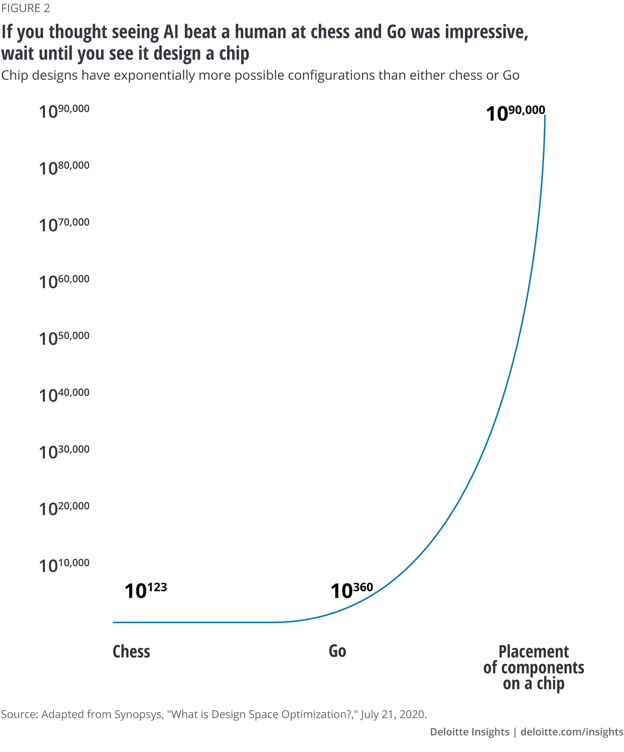
RL turns physical chip design into a graph optimization “game.” It’s the same technology Google used to defeat the human champion in the strategy board game Go, which is even more complicated than chess and was thought to be beyond AI’s abilities. Physical chip design is exponentially more complex still (figure 2), but RL tackles it in the same way. It trains on thousands of “games”—chip floor plans, which simulate chip designs to find the best PPA arrangements. The AI-generated floor plans are reinforced by a mix of rewards from the human designers for designs that optimize PPA, such as those that reduce wire length, congestion, density, power consumption, and area,13 and punishments for suboptimal designs. These reinforcements improve the RL system over time, teaching it to generate better designs autonomously.14

The combination of GNNs and RLs is delivering PPAs whose performance equals or exceeds those produced by experienced designers, using fewer human engineers and in far less time. Some recent real-world results:

  • MIT’s AI tool developed circuit designs that were 2.3 times more energy-efficient than human-designed circuits.15
  • MediaTek used AI tools to trim a key processor component’s size by 5% and reduce power consumption by 6%.16
  • Cadence improved a 5 nm mobile chip’s performance by 14% and reduced its power consumption by 3%, using AI plus a single engineer for 10 days instead of 10 engineers for several months.17
  • Alphabet consistently produces chip floor plans that exceed experienced human designers in PPA metrics in six hours instead of weeks and months.18
  • NVIDIA used its RL tool to design circuits 25% smaller than those designed by humans using today’s EDA tools, with similar performance.19

The bottom line

Major chipmakers and designers are using the latest AI to design chips today, even at advanced nodes. In fact, some chips are getting so complex that advanced AI may soon be required. For instance, the largest chip design from Synopsys contains more than 1.2 trillion transistors and 400,000 AI-optimized cores.20

Advanced AI is also becoming available through cloud-based EDA services, expanding the addressable market. Once on the cloud, it is available to smaller companies with less technical skill and compute power, not just experts and market leaders.21

The biggest semi companies could even use advanced AI to develop new services to monetize. By expanding their GNN and RL capabilities, these companies could not only generate their own designs but also offer design and co-design services to their top customers, including co-developing vertical-specific chips.

AI can be useful to the chip industry for more than just designing chips. For example, it can be used to improve fault detection by visual inspection of wafers by almost nine times.22 It can also allow chip companies to address supply chain challenges such as managing a network of outsourced semiconductor assembly and test providers.23

For a few years, there have been chips designed for AI; now, there are chips designed by AI. What comes next? AI will likely start co-designing both the hardware and the software that powers AI itself—creating an innovation flywheel that might power the 21st century.

  1. Deloitte Global estimates that the market for third-party AI chip design software from the major vendors was valued at about US$150 million in 2022 and will be worth over more than US$200 million in 2023. Further, we estimate that the internal use of AI design tools by large chip companies is worth about the same size.

    View in Article
  2. Deloitte Global estimated growth rate from public statements by EDA companies and analyst reports.

    View in Article
  3. World Semiconductor Trade Statistics, “The World Semiconductor Trade Statistics (WSTS) has released its new semiconductor market forecast generated in August 2022,” press release, August 22, 2022.

    View in Article
  4. Global Market Insights, Electronic design automation market report, 2020.

    View in Article
  5. Elements of machine learning have been included in EDA tools for several years, but the use of advanced AI technologies such as GNNs and RL is new, and has dramatically increased the effectiveness of AI in chip design.

    View in Article
  6. John Ciacchella et al., 2022 semiconductor industry outlook, Deloitte, 2022.

    View in Article
  7. International Business Strategies (IBS), 2021.

    View in Article
  8. Ciacchella et al., 2022 semiconductor industry outlook.

    View in Article
  9. Deloitte Global used both top-down (most current reported direct employment by country/region) and bottom-up (number of employees reported by all the large companies) approaches to estimate the 2021 global semiconductor industry direct employment. Given that the industry will be 80% larger by revenues in 2030 but will also be less concentrated than it is today (therefore needing more workers per dollar of revenue), we assume that it will need roughly 50% more employees.

    View in Article
  10. Abid Ali Awan, “A comprehensive introduction to graph neural networks (GNNs),” DataCamp, July 2022.

    View in Article
  11. For an accessible explanation of why neural networks struggle to analyze graph data, and why GNNs are better, see: Ben Dickson, “What are graph neural networks (GNN)?,” VentureBeat, October 13, 2021; for a more technical view, see DataCamp, “A comprehensive introduction to graph neural networks (GNNs),” July 2022.

    View in Article
  12. Dickson, “What are graph neural networks (GNN)?

    View in Article
  13. Ed Targett, “AI outperforms humans in chip design breakthrough,” The Stack, June 10, 2021.

    View in Article
  14. BBC News, “Go master quits because AI ‘cannot be defeated’,” November 27, 2019.

    View in Article
  15. Will Knight, “Need to fit billions of transistors on a chip? Let AI do it,” Wired, July 9, 2021.

    View in Article
  16. James Morra, “Cadence taps AI technology to speed up system design,” Electronic Design, June 13, 2022.

    View in Article
  17. John Koon, “Improving PPA with AI,” Semiconductor Engineering, May 12, 2022.

    View in Article
  18. Azalia Mirhoseini et al., “A graph placement methodology for fast chip design,” Nature 594 (2021): pp. 207–12.

    View in Article
  19. Rajarshi Roy, Jonathan Raiman, and Saad Godil, “Designing arithmetic circuits with deep reinforcement learning,” NVIDIA Developer, July 8, 2022.

    View in Article
  20. Stelios Diamantidis, “Why now is the time to create an AI strategy for chip design,” Synopsys blog, June 16, 2021.

    View in Article
  21. Jeff Loucks, Artificial intelligence: From expert-only to everywhere, Deloitte Insights, December 11, 2018.

    View in Article
  22. Tobias Schlosser et al., “Improving automated visual fault inspection for semiconductor manufacturing using a hybrid multistage system of deep neural networks,” Journal of Intelligent Manufacturing 33 (2022): pp. 1099–1123.

    View in Article
  23. Deloitte, "Supply chain and network operations: Enterprise technology and performance," accessed October 26, 2022. 

    View in Article

The authors would like to thank Ariane Bucaille, Gillian Crossan, Dan Hamling, and Karthik Ramachandran for their contributions to this chapter.

Cover image by: Jaime Austin and Sofia Sergi

Semiconductor Industry Trends and Services

The Deloitte Semiconductor practice brings the strength of our multiservice, global organization to help with the most critical issues while understanding the complexities, nuances, and uniqueness of the industry and their implications for your organization. Additionally, our relationships with some of the world’s leading companies make productive, traditional alliances possible, but we go above and beyond to form connections matched to your unique ambitions. This helps you scale exponentially and tap into the value potential of mega technology trends to thrive in a constantly shifting market.

Jeff Loucks

Jeff Loucks

Executive director
Christie Simons

Christie Simons

Global Semiconductor Center of Excellence Leader | US A&A TMT Leader | Audit & Assurance Partner

Subscribe

to receive more business insights, analysis, and perspectives from Deloitte Insights