Semiconductor sustainability: Manufacturing change has been saved

Perspectives
Semiconductor sustainability: Manufacturing change
Strategies for reducing direct environmental impact
The seemingly exponential growth of the semiconductor industry has not only increased demand for more powerful chips, but more sustainable fabrication and assembly as well. At the same time stakeholders are calling for more effort to curb emissions and other environmental impacts, manufacturers are seeing how sustainability enhancements can increase efficiency and cost effectiveness.
Adding these conditions to the number of recent government policies and incentives that reward or require improved manufacturing sustainability creates a near ideal scenario for investing in sustainable solutions, technology, and processes for semiconductor manufacturing.
Context:
Many of the world’s leading semiconductor manufacturers publicly announced sustainability goals in recent years. While each has pursued their own set of initiatives to move toward achieving these goals, many initial efforts have focused on relatively accessible progress such as procuring renewable energy where possible. For example, 93% of Intel’s energy needs were met by renewables as of its 2022-23 fiscal year.1
The imperative to further improve the industry’s sustainability (see drivers below) continues to intensify, accentuated by the continued growth of the industry and the greater energy demands of manufacturing the latest generation chips. Thankfully, new technologies, processes, and incentives are becoming available to enable further improvements in the environmental footprint of chip fabrication and assembly. We can thus anticipate improved environmental performance from both the next generation of plants and from retrofitting and upgrades of existing facilities. A targeted transformation of chip manufacturing with adoption of the latest technologies, processes, and approaches can reduce the intensity of energy, water, and process gas use significantly.
Explore the conditions driving demand for more sustainable technologies and processes in semiconductor chip manufacturing.
How are market drivers and investments in increased chip manufacturing sustainability impacting semiconductor manufacturers?
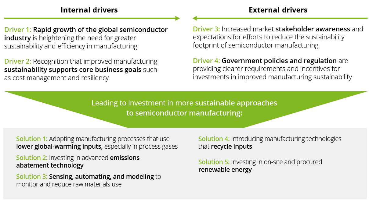
From Deloitte’s experience, we see the varied pressures to reduce the lifecycle energy needs of semiconductor products being expressed via four main drivers:
Driver #1: Rapid growth of the global semiconductor footprint
The rapid expansion of semiconductor chip manufacturing is leading to a growing environmental footprint which can be at odds with the stakeholder sustainability expectations, publicized sustainability goals, and business incentives (see driver #2 below). This is amplified further by the fact that manufacturing the most advanced semiconductors has an even greater environmental impact than past generations of devices. Advanced node technologies (sub-10nm) have longer manufacturing processes, which increase the sustainability impact. Moving from a mature technology such as 28nm to advanced node manufacturing at 2nm needs 3.5x as much energy, 2.3x as much water, and 2.5x as many greenhouse gases.2 Broad recognition of—and concern about—these trends is further accentuating the sense of urgency to reduce the chip manufacturing sustainability footprint.
Driver #2: Alignment with core business goals
There is growing understanding among semiconductor sector executives that improving sustainability can be directly supportive of significant business goals—and help drive a competitive advantage. Many semiconductor manufacturers and their business customers have set explicit goals for reducing their Green House Gas (GHG) emissions and other sustainability impacts. Given that the majority of such impacts are concentrated in the fabrication and assembly process steps, progress toward these goals requires addressing impacts from these processes. Further, it has come to be understood that addressing manufacturing process sustainability can directly support business fundamentals: growing scarcity of key inputs such as water and energy in the countries where manufacturing plants are located means that increased efficiency in their use can support business growth and operational continuity. On-site solar power for example tends to buffer grid outages and can reduce energy costs. Recycling water can help address local community concerns about water availability and cost. Similarly, efforts to reduce volume or recycle water and other manufacturing inputs such as gases often have a cost-reduction benefit. In a potentially slowing global economy, these cost-favorable drivers serve to further bolster the case for investments in sustainability-enhancing efficiency improvements.
Driver #3: Increased awareness and expectations of market stakeholders
Recent years have seen the combination of semiconductors becoming ever-more prevalent in our economies and daily lives, with growing stakeholder understanding of the environmental impacts of chip manufacturing such as water use, energy use, and process use of gases with strong global warming impacts. This is leading stakeholders (including customers, investors, and even staff) to demand a redoubling of efforts to reduce the semiconductor manufacturing sustainability footprint. Investors are starting to pay attention to how much energy, water, and high Global Warming Potential (GWP) process gases are used per unit of revenue.3
Driver #4: Regulation and government incentives
As described in other articles in Deloitte’s Semiconductor Sustainability series, a range of government policies and incentives—especially in the US and Europe— is driving a transition to greater energy efficiency, which in turn is supporting a shift toward greater sustainability in the manufacture of semiconductors. In the US, incentives for energy efficiency have recently been strengthened by the Inflation Reduction Act which includes significant grants and other incentives for energy efficiency in buildings, corporate fleet electrification, and renewable energy expansion (among other areas.) The recently passed California Climate Corporate Data Accountability Act (SB 253) as well as the European Union’s Corporate Sustainability Reporting Directive (CSRD) broadly require companies to publicly disclose and verify their greenhouse gas emissions, thereby creating transparency incentives to reduce energy use and the related emissions. When these incentives are viewed in combination with the CHIPS Act, which is prompting semiconductor companies to investigate opportunities to expand their R&D, manufacturing, assembly, packaging, and testing in the United States, one can anticipate an increasing investment in more efficient semiconductor plants.
In response to these drivers, semiconductor companies are further investing in the reduction of environmental impacts from their manufacturing operations. What targeted approaches are they taking to improve sustainability and position their businesses for the future?
Solution #1: Adopting manufacturing processes that use lower global-warming inputs
Semiconductor manufacturers are investing in new plants and retrofitting existing plants with processes that make use of raw materials such as chemicals and gasses with lower emissions and lower GWP.
Established chip manufacturing processes use several gases that have very high GWP, especially fluorinated gases such as perfluorocarbons (PFCs), hydrofluorocarbons, nitrogen trifluoride (NF3), and sulfur hexafluoride. In the majority of established manufacturing processes up to 80% of fluorinated gases are released into the atmosphere at the end of the process.4 There has been progress in finding alternative gases—for example, replacing PFCs with NF3, which has a lower GWP.5 Tokyo Electron Limited (TEL) announced a new high-aspect ratio etch process that significantly reduces both energy and the CO2 footprint of the etch. The etch is performed at cryogenic temperatures and uses an alternative chemistry to the current process. TEL claims that the etch is 2.5x faster, uses 43% less power, and reduces GHG by 83%.6
Samsung Semiconductor is also developing process gas with lower global warming potential. This alternative gas has been developed to replace PFCs, one of the most potent greenhouse gases, used in the four major semiconductor processing steps—etching, diffusion, chemical vapor deposition, and metallization. PFCs have been replaced in processing several products since 2018.7 Nevertheless, finding and introducing alternative gases is a lengthy process that tends to yield incremental improvements. This points to the growing importance of the next solution: abatement.
Solution #2: Investing in advanced emissions abatement technology
Given the challenges in identifying and introducing lower GWP process gases, abatement of high GWP process gas emissions is a key solution being adopted ever more widely in semiconductor manufacturing plants. Capturing and destroying (for example, by burning or chemical conversion) as much of the high GWP process gases is key; abating 99% of NF3 is now possible.8 Samsung Semiconductors has introduced the Regenerative Catalytic System (RCS), a facility on the rooftop that handles all the process gas with catalysts. By treating process gas at a low temperature, Samsung Semiconductor’s RCS tends to use less fuel and emit fewer air pollutants compared to point-of-use facilities widely used by other manufacturers. Samsung also announced that they have developed a more durable catalyst for their RCS with up to 95% processing efficiency.9
Solution #3: Sensing, automating, and modeling to monitor and reduce raw materials use
Increasingly, internet of things technologies are being used to sense and optimize individual manufacturing machinery and process stages to minimize use and leakage of energy, gases, water, and chemicals used in manufacturing processes. In many cases, leaks can be detected, and systems can be idled or powered down when not in use. For manufacturing process stages that are hard to access or monitor in real time, process modeling and use of digital twins can be used. While fully upgrading a decade-old chip manufacturing plant can cost hundreds of millions of dollars, the gains in sustainability and operating costs increasingly justify it.
Building information management (BIM) is a technology increasingly used to design and manage the performance and sustainability of semiconductor manufacturers’ buildings (as, indeed, it is in other industries). BIM is the process of creating and managing information on a construction process, and by incorporating this additional dimension, the virtual model is designed to depict not just the physical, temporal, and cost-related aspects of the building but also its environmental and social implications. Consequently, this could become a valuable resource for evaluating how the building affects its surroundings and community and for recognizing opportunities for enhancement.10
Solution #4: Introducing manufacturing technologies that recycle inputs
Logically, one of the most effective approaches to reducing the volume of inputs used in a manufacturing process is to find ways to feed them back into the process multiple times. Semiconductor manufacturers are following this approach with several inputs—for example, with the previously discussed process gases and also with water (around 76% of the water use in the semi industry is for the manufacturing process).11 The scale of adoption of this approach is illustrated by the fact that Intel returned more than 80% of its water for reuse in the manufacturing process,12 while chipmakers across Taiwan report an average of 85% water recycling between 2016 and 2020.13 In Europe, Infineon has announced that at their production sites in Dresden (Germany), Regensburg (Germany), and Villach (Austria), significant amounts of heat are already being generated from integrated energy recycling via the recovery of exhaust heat, thereby significantly reducing the demand for energy to produce heating power.14
Solution #5: Investing in onsite and procured renewable energy
One of the most widely adopted approaches to increased sustainability among semiconductor manufacturers has been a shift to the use of renewable energy. This has been composed of both installation of onsite solar power and procurement of renewable energy from electrical utilities. The availability and cost of onsite solar generation technologies and limited availability of renewable energy from energy utilities slowed adoption initially. However, each of these bottlenecks has been easing in recent years, with renewable energy being more available in fabrication countries such as Taiwan and the Philippines as well as the United States.
Since 2015, NXP Semiconductors has steadily increased their use of electricity from renewable sources. In 2022, 35% of overall electricity use was from renewable energy sources, while their Nijmegen wafer fab in the Netherlands runs on 100% renewable electricity.15 In June 2018, Samsung announced their goal to use 100% renewable energy for all sites in the United States and China by 2020. They achieved their goal a year ahead of schedule, replacing all electricity with renewable energy by 2019.16 Meanwhile, in their 2021 fiscal year, Infineon switched to purchasing 100% green electricity for its sites in Europe. In the 2022 fiscal year, the North American site in Austin (Texas, US) followed suit.17
How can you capitalize on semiconductor industry disruption to drive competitive advantage? Take a deeper look at industry trends and solutions in our Semiconductor Sustainability series.
Conclusion
The highly complex and costly process for manufacturing and assembling semiconductor products has presented challenges for addressing its sustainability footprint. However, a combination of clear business drivers and the emergence of technically and economically feasible approaches is making the sustainability footprint of semiconductor manufacturing more addressable now than ever before. This is fortunate given the anticipated dramatic growth in the use of semiconductors as adoption of new technologies, such as 5G and AI, continues seemingly unabated.
Get in touch


Endnotes
1 Intel, 2022–23 corporate responsibility report, 2023.
2 Marie Garcia Bardon and Bertrand Parvais, “The environmental footprint of logic CMOS technologies,” Imec, December 17, 2020.
3 Mike Czerniak, “The time is now: Sustainable semiconductor manufacturing,” Semiconductor Digest (November 2021): pp. 16–19.
4 United States Environmental Protection Agency, “Electric Power Systems Partnership – Semiconductor Industry,” accessed December 19, 2023.
5 Czerniak, “The time is now: Sustainable semiconductor manufacturing.”
6 Dean Freeman, “Solving semiconductor greenhouse gas chemistry challenges,” 3D InCites, September 20, 2023.
7 Samsung Semiconductor, “Climate Action,” accessed December 18, 2023.
8 Bardon and Parvais, “The environmental footprint of logic CMOS technologies.”
9 Samsung Semiconductor, “Climate Action.”
10 The BIM Engineers, “From 3D BIM to 7D BIM,” TBE Blog, June 8, 2023.
11 Ibid.
12 Intel, “Intel achieves net positive water in 3 countries,” press release, July 13, 2022.
13 Chris Jones, “Water supply challenges for the semiconductor industry,” Semiconductor Digest, October 24, 2022.
14 Infineon, “Energy efficiency and climate protection,” accessed December 18, 2023.
15 NXP, “Energy,” accessed December 18, 2023.
16 Samsung Semiconductor, “Climate Action.”
17 Infineon, “Energy efficiency and climate protection,” accessed December 18, 2023.
Recommendations

Semiconductor | Deloitte US
Deloitte's semiconductor consulting practice can solve critical issues. Explore semiconductor industry trends, from M&A to cloud to IoT, to help drive growth.