How GenAI is transforming the semiconductor value chain has been saved

Perspectives
How GenAI is transforming the semiconductor value chain
New applications supercharge semiconductor innovation
As semiconductor demand remains steady, chip manufacturers are challenged to develop faster, cheaper, higher-capacity chips. Is GenAI the answer to supercharging semiconductor innovation and accelerating chip design and manufacturing? Dive into the top applications for generative AI in semiconductor manufacturing.
GenAI fuels new semiconductor business models
Semiconductors power every conceivable electronic device—putting chip design at the core of technological innovation. Under constant pressure to develop faster, cheaper, higher-capacity chips, manufacturers have pushed traditional design, manufacturing, and verification to new levels. Meanwhile, the industry’s appetite for semiconductor innovation shows few signs of slowing.
Enter GenAI. Used to supercharge different aspects of how semiconductors are created, with transformative effects on nearly everything from iterating to prototyping to manufacturing. The technology is especially adept at adding intelligence to large, complex data models and accelerating the planning, development, and execution of chip design and manufacturing.
The industry knows an opportunity when it sees it: Semiconductor giants invested approximately $300 million in AI tools for chip design in 2023, a total expected to rise to $500 million by 2026. And 72% of the semiconductor professionals Deloitte polled in 2023 believe that GenAI’s impact on the industry will be “high to transformative.” AI is a lot more than just a new tool; it can be a foundational element with the power to open up entirely new opportunities.
Semiconductor value chain
Common semiconductor industry applications
GenAI can be used to accelerate and differentiate product designs, improve operations, and proliferate leading practices throughout the semiconductor industry value chain, especially in these areas of the business:

- Planning: Supply chain forecasting. Generate more accurate schedules and forecasts while optimizing process flows.
- R&D: Research augmentation. Use custom mixed-language models to help develop knowledge bases, notes, and communication records. All are fully searchable, facilitating sharing of leading practices and discovery of reference designs and customer intellectual property.
- Design: Design generation. Rapidly iterate to improve existing designs or discover entirely new ones. Optimize performance based on criteria including power consumption, performance, location, and manufacturability, saving both time and money.
- Manufacturing: Anomaly and defect detection. Generate synthetic data for use in downstream defect detection algorithms. Automatically identify rare failure modes and quantify them more accurately.
- Manufacturing: Process simulation. Use training data from sensors, process logs, and other sources to generate digital twins that can simulate sorting, assembly, testing, and other complex manufacturing processes. Build capacity models and flows that can maximize productivity and optimize equipment and resource use.
- Operations: Streamlined legal contract review. Verify important legal clauses in contracts, highlight issues, suggest changes, and revise contract language. Extract critical information pertinent to individual contracts or intellectual property. Automatically pull critical dates (payments, deadlines, renewals), populate calendars, and send notifications when action is required.
- Pre-sales: Product selection and search. Assist semiconductor field application engineers with product selection, search, part explanation, and citation for customers. Help design engineers find the optimal engineering part or SKU for end-circuit design.
Top opportunities in chip manufacturing
While GenAI is relatively new to the industry, our survey respondents saw high potential for its use throughout the semiconductor business; this reflects the interest for GenAI across the semiconductor value chain with slightly heavier expectations of value lying within core engineering chip design and manufacturing, operations, and maintenance.
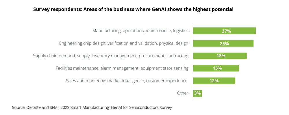
Within the manufacturing, operations, and maintenance function, respondents saw the highest potential value for GenAI in three areas: analysis of/insight into processes and equipment (28%), diagnostics and troubleshooting of processes and equipment (25%), and predictive maintenance (18%).
For GenAI in engineering, respondents saw the most potential in verification and validation test case development (29%), architecture and design scenarios (22%), and detailed physical design and layout options (17%). One example: context aware GenAI tools that use conversational intelligence and natural language prompts to eliminate much of the grunt work of RTL generation and verification.
The future of GenAI in semiconductor manufacturing
Today there are many GenAI-enabled productivity and efficiency improvements that can help designers, researchers, and developers accelerate low-risk workflows while keeping human specialists in the loop. Beyond this low-hanging fruit, more and more automation is possible, reducing costly human involvement while increasing the deployment risks. For example, GenAI could be used to generate scanning electron microscope images of rare defect modes immediately. These generated images can then be used to train downstream defect detection algorithms. Longer-term opportunities will likely flow from systemwide workflow changes such as material design, circuit path finding, fab simulation, operational optimization, and dynamic pricing via simulated agents, which require significant domain expertise and major investment; such heavy investment allows for significantly larger market leading opportunities with higher possible return on investment.
Of all GenAI use cases, text generation, summarization, translation, and classification are the most developed, followed by applications such as time-series forecasting and signal processing.
Emerging issues
GenAI has the potential to revolutionize the semiconductor industry—dramatically improving efficiency and accuracy, helping to maximize quality, speeding product development, and opening new areas of innovation. But before embarking on any GenAI journey, it’s important to carefully consider the potential risks, including:
- Cost: Building custom models for generating circuit design, testing plans, and synthetic data can be expensive compared to manual execution. Ongoing costs for very large models can also outweigh the speedy benefits of automation.
- Accuracy: Contrary to popular belief, GenAI may not always deliver outputs with the same quality and accuracy of humans using more traditional methods. AI models can generate content with errors, inconsistencies, and hallucinations. The solution: Keep humans in the loop. Use GenAI to augment rather than replace human contributions—validating everything from designs and testing to code.
- Bias and privacy: Consider ethical issues when working with human-centered applications such as HR or sales and marketing. Mandatory human review can help ensure that all data is sanitized, personally identifiable information removed, guardrails installed, and results validated.
How Deloitte can help
In the semiconductor business, managing impossibility and navigating uncertainty are just part of the job. You need collaborators that understand the complexities and nuances of this unique industry—and their implications for your organization. Deloitte’s multitalented, multidisciplinary tech pioneers and GenAI specialists can help you identify new ways to sustain growth, gain a competitive edge, and power a more promising future.
Contacts


Recommendations

2024 semiconductor industry outlook
Trends and predictions for a cyclical industry

2023 Semiconductor Transformation Study
Business transformation in the semiconductor industry